There is a local version available of this page. Change to the local version?
United States

Semiconductors

Stress Analysis for Semiconductor Raw Materials

<< Back to Raw Materials for Semiconductors

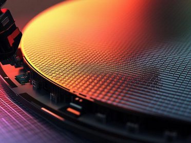
We propose a multifaceted stress evaluation solution using a Raman spectrometer boasting high wavenumber and spatial resolution, along with cathodoluminescence (CL).

Browse all applications

Microscopic Raman spectrometer LabRAM Odyssey

  • Industry's highest level* stress resolution (*according to our research in 2022)
  • Capable of mapping up to 12 inch wafers
  • Temperature control holder can be used (please consult us separately regarding sample size)


AFM (atomic force microscope) Raman XploRA Nano

  • Acquire physical information by AFM and chemical information by Raman simultaneously
  • Stress distribution analysis on the outermost surface on the order of nm is possible.

Pedido de Informação

Você tem alguma dúvida ou solicitação? Utilize este formulário para entrar em contato com nossos especialistas.

* Esses campos são obrigatórios.