It is possible to analyze the crystallinity, number of layers, etc. of minute regions of two-dimensional materials, which are next-generation semiconductor materials.
Cathodoluminescence Solutions for Electron Microscopy
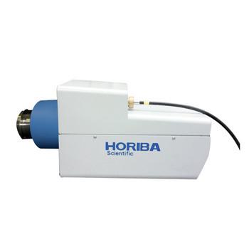
Compact Hyperspectral Cathodoluminescence
Versatile Hyperspectral Cathodoluminescence
Raman Photoluminescence & Cathodoluminescence
AFM-Raman for Physical and Chemical imaging
Você tem alguma dúvida ou solicitação? Utilize este formulário para entrar em contato com nossos especialistas.
You might also like to know