It is possible to analyze the crystallinity, number of layers, etc. of minute regions of two-dimensional materials, which are next-generation semiconductor materials.
Cathodoluminescence Solutions for Electron Microscopy
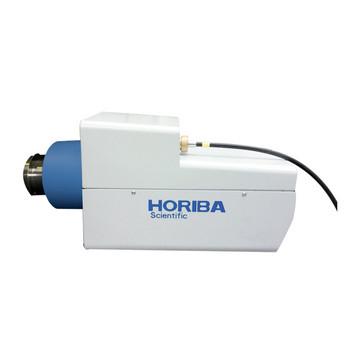
Compact Hyperspectral Cathodoluminescence
Versatile Hyperspectral Cathodoluminescence
Raman Photoluminescence & Cathodoluminescence
AFM-Raman for Physical and Chemical imaging
如您有任何疑問,请在此留下詳細需求或問題,我們將竭誠您服務。
You might also like to know