There is a local version available of this page. Change to the local version?
United States

Semiconductors

Crystal Defect Analysis for Semiconductor Raw Materials

<< Back to Raw Materials for Semiconductors

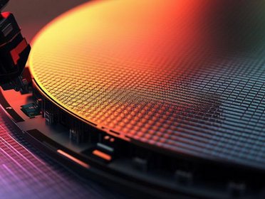
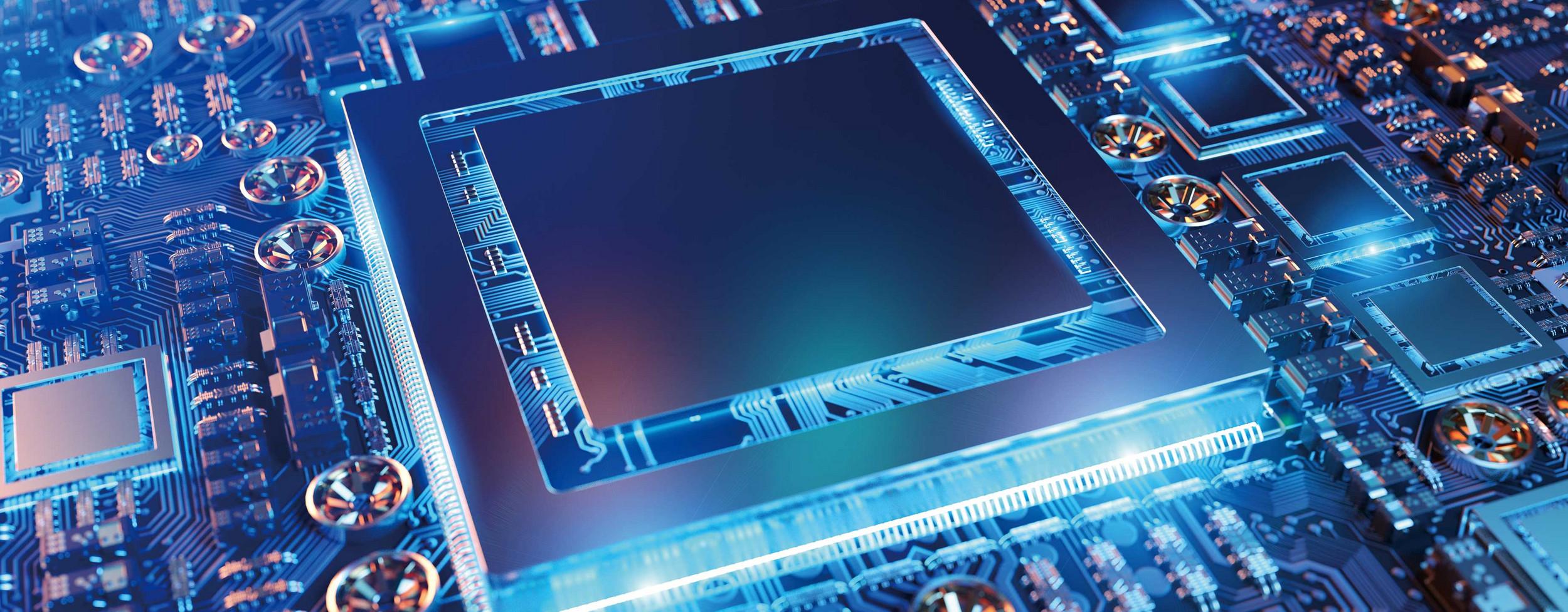
Reducing defects and precisely controlling impurities have become increasingly important in semiconductor devices for high-speed communication. We will introduce analysis cases illustrating this.
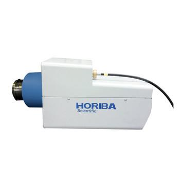
Cathodoluminescence measurement system HORIBA CLUE series

  • Can be added to existing electron microscopes
  • Compatible with measurements at ultraviolet to near-infrared wavelengths (200 to 2,100 nm)
  • SEM integrated high range CL imaging device (Imaging CL) can also be proposed.

AFM (atomic force microscope) Raman XploRA Nano

  • Acquire physical information by AFM and chemical information by Raman simultaneously
  • Stress distribution analysis on the outermost surface on the order of nm is possible.

Browse all applications related to Crystal defect analysis

留言諮詢

如您有任何疑問,请在此留下詳細需求或問題,我們將竭誠您服務。

* 這些欄位為必填項目。