Imagine squeezing more powerful chips onto a single wafer. That's the promise of large wafer semiconductors, pushing the boundaries beyond the standard 300 mm diameter size towards 450 mm.
Larger wafers mean more chips per run, boosting efficiency and potentially lowering costs per chip. It also means simpler, faster production with fewer steps, streamlining production and potentially improving chip quality.
And large wafer semiconductors mean paving the way for even more complex and powerful chips. In fact, these are used for high-performance computing, artificial intelligence, and other areas demanding high power and density.
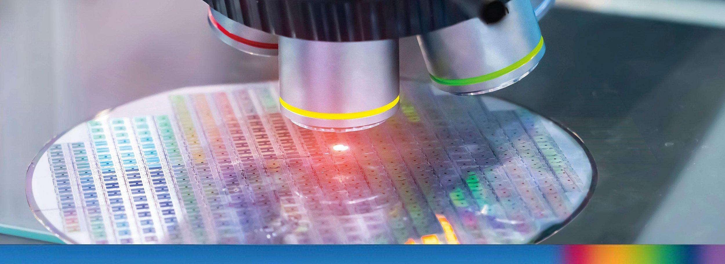
But challenges exist. Developing and using this technology isn’t easy, requiring big investments from manufacturers. And working with these requires overcoming technical hurdles in handling, processing, and testing. That’s where HORIBA comes in. Its Standard Microscopy Spectroscopy solutions can detect defects on these large wafers using oversized platforms for analysis.
Add Spectroscopy to ANY Microscope
Do you have any questions or requests? Use this form to contact our specialists.