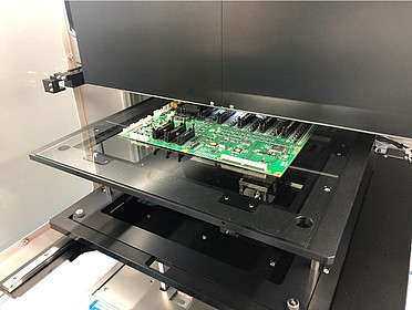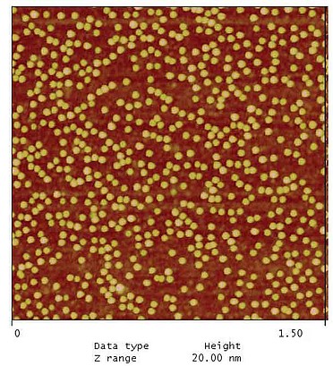
HORIBA has revolutionized thin film measurement by integrating its proprietary spectroscopic ellipsometer with fully automatic measurement technology. This innovation has led to the creation of a fully automated thin film measurement system that supports multi-point measurement and mapping capabilities, complete with automatic transport. Capable of swift and precise measurements, this system accurately determines the thickness and optical constants of various thin films and multilayer films on various wafer substrates.
Fully Automated Thin Film Inspection System
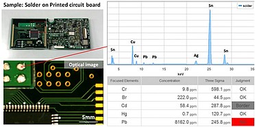
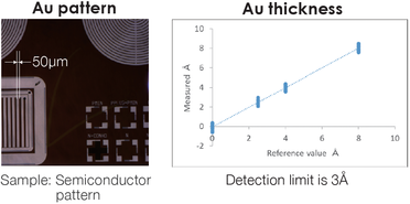
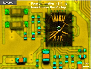
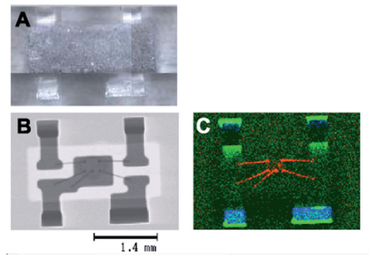
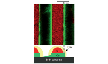
From impurities and contaminants analysis to defect analysis and process control, HORIBA offers a wide range of analytical instruments applicable to a large range of semiconductor materials, including silicon, germanium, gallium arsenide, silicon carbide, gallium nitride and others. Our robust and reliable Raman spectrometers, X-ray Fluorescence microscopes, spectroscopic ellipsometers, elemental analyzers and particle size analyzers will help you to take your semiconductor processes to the next level. Learn how HORIBA technologies and application experts can help you to maintain the highest level of productivity.
![]()
У вас есть вопросы или пожелания? Используйте эту форму, чтобы связаться с нашими специалистами.


")