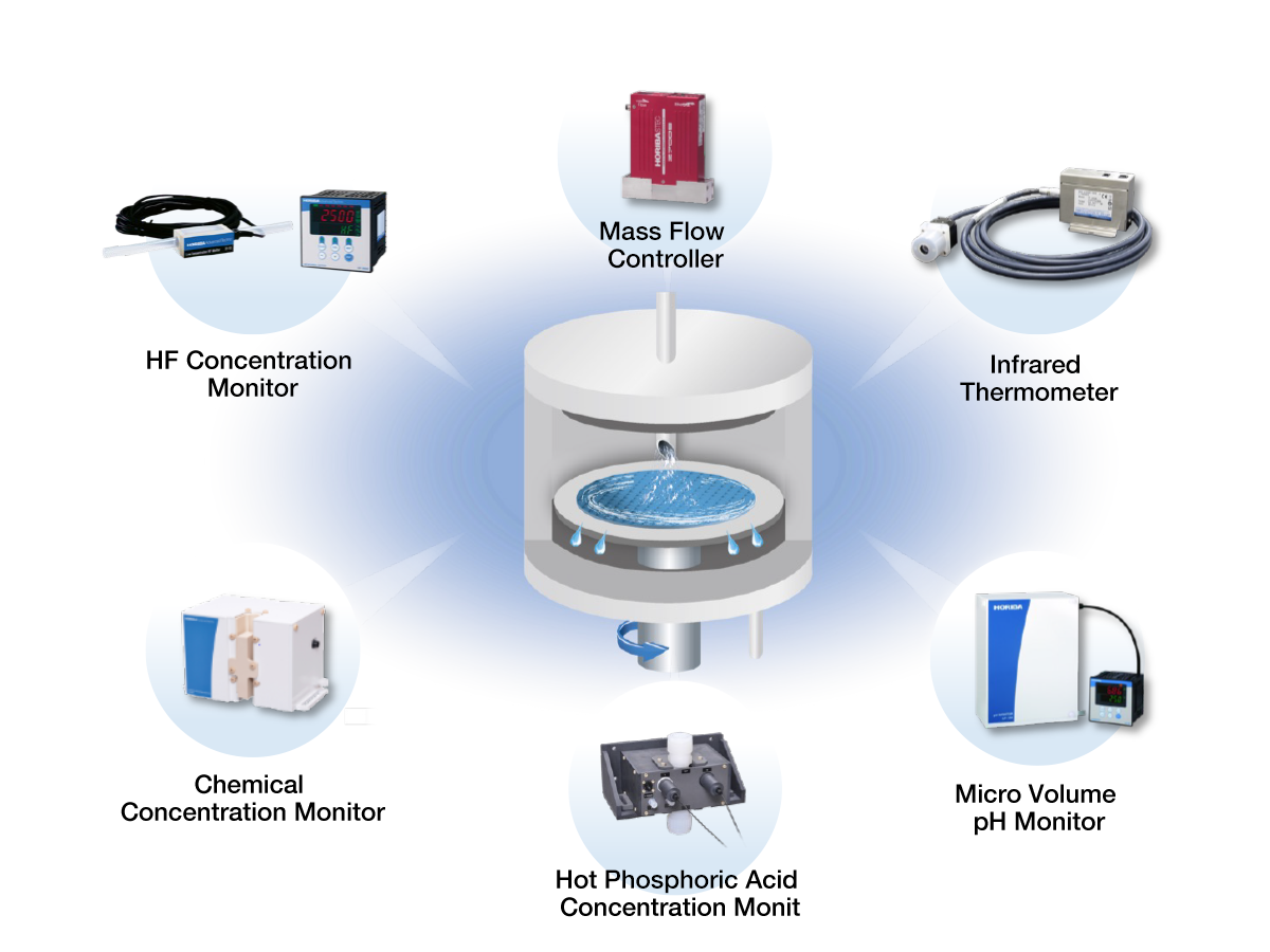
After chemical treatment of semiconductor wafers for cleaning, etching or stripping applications, or MEMS device KOH/HF etching applications, the process chemicals should be completely removed from the surface in order to stop the chemical reaction and take away chemical residues. Chemistry is still covering the wafer surface, in particular within recess structures of the topology (moats, trenches) resulting in continuation of the chemical process outside the bath. This is critical for etch applications, since over-etching might occur destroying the pattern and causing significant yield loss. Custom plastic tanks, PFA tanks are the common choices for quick dump rinsing steps.
Three types of rinsing are used in semiconductor manufacturing, depending on the tool type and application:
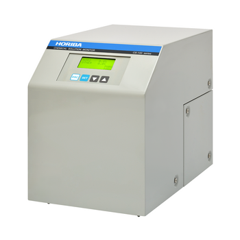
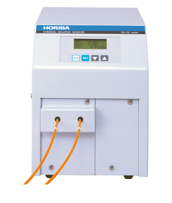
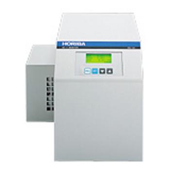
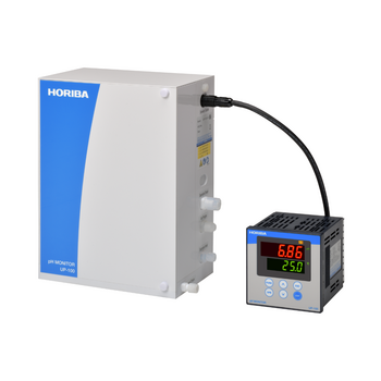
Stand-alone Type Chemical Concentration Monitor
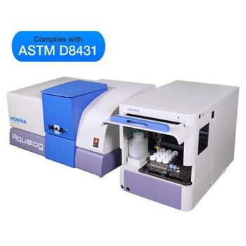
A Simple, Fast, “Column Free” Molecular Fingerprinting Technology
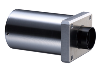
High-Accuracy Infrared Thermometer [Built-in type]
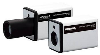
High-Accuracy Infrared Thermometers [Stationary type]
마이크로 볼륨 pH 모니터
HORIBA제품의 자세한 정보를 원하시면, 아래의 양식에 내용을 입력을 부탁드립니다.