<< Back to Raw Materials for Semiconductors
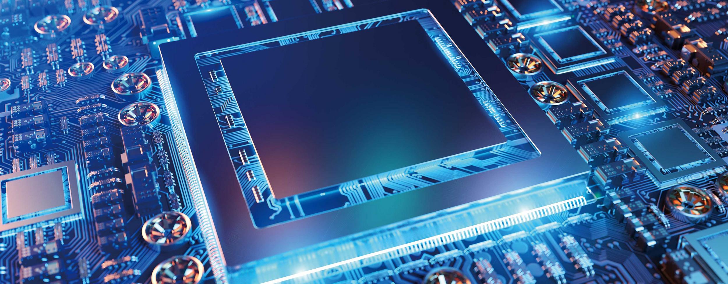
Silicon material continues to be mainstream of next-generation packages that integrate miniaturized chips and chiplets, making it possible to create more complex integrated systems as well as less expensive. HORIBA will contribute with its measurement technology for film thickness measurement, stress analysis, elemental analysis, and foreign material analysis of silicon materials.
Film Thickness and Quality | Stress Analysis | Elemental Analysis | Foreign Object Detection/Analysis
In the advancement of thin film technology through miniaturization, we propose solutions for achieving high film deposition control, such as in-situ evaluation during the film deposition process and evaluation of thin films at the Ångström order level.
Membrane information obtained using a spectroscopic ellipsometer
We propose a multifaceted stress evaluation solution using a Raman spectrometer boasting high wavenumber and spatial resolution, along with cathodoluminescence (CL).
Defects in wafers can also be caused by foreign matter, and we will introduce a method of microscopic elemental analysis to identify the cause of defects.
HORIBA제품의 자세한 정보를 원하시면, 아래의 양식에 내용을 입력을 부탁드립니다.
Spectroscopic Ellipsometer from FUV to NIR: 190 to 2100 nm
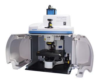
Raman Microscope
Confocal Raman Microscope
Raman Spectrometer - Confocal Raman Microscope
Confocal Raman & High-Resolution Spectrometer
AFM-Raman for physical and chemical imaging
AFM-Raman for Physical and Chemical imaging
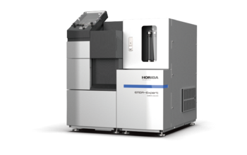
탄소/황 분석기 (인덕션 퍼니스 타입)
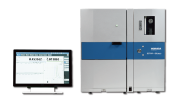
산소/질소/수소 분석기
산소/질소/수소 분석기
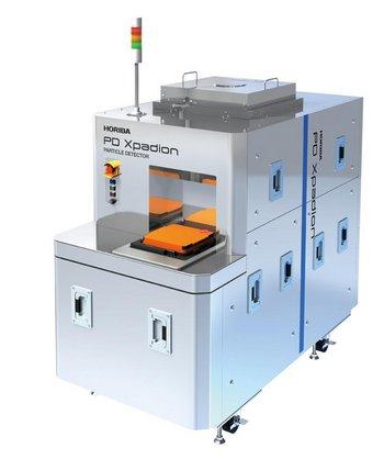
Reticle / Mask Particle Detection System