PL spectrum and PL life can be obtained with one device, allowing multifaceted evaluation.
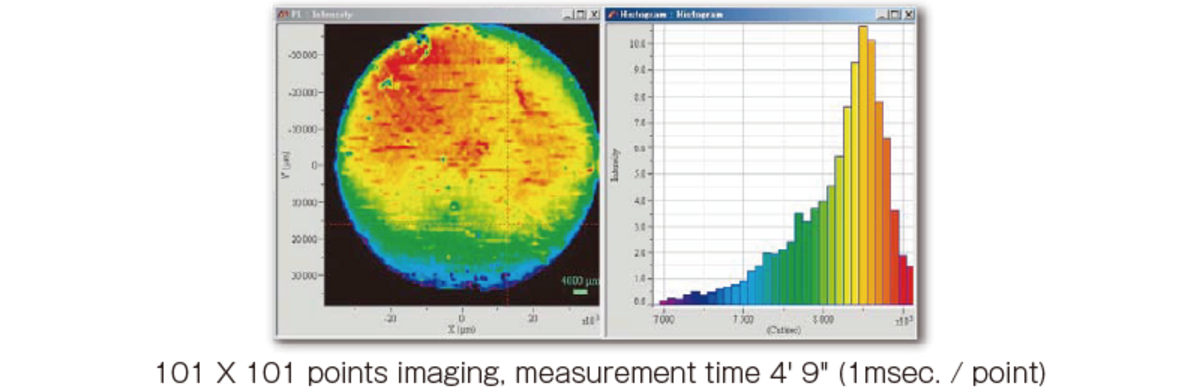
Mapping image of photoluminescence peak intensity, wavelength, and half-width of a 2-inch compound semiconductor wafer
Obtain PL information for over 10,000 items in minutes. The peak wavelength distribution is expressed as a histogram.
101x101 points imaging, measurement time 4' 9 (1msec. point)
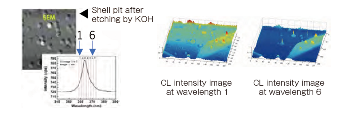
Mixed (edge and screw) dislocations are observed in CL image 1, and edge dislocations are observed in CL image 6. In this way, defect types can be evaluated by displaying three-dimensional intensity images based on wavelength.
With time-resolved measurement, it is possible to read slight differences in luminescent components that cannot be read in a steady PL spectrum.
Cathodoluminescence Solutions for Electron Microscopy
Compact Hyperspectral Cathodoluminescence
Versatile Hyperspectral Cathodoluminescence
Raman Photoluminescence & Cathodoluminescence
AFM-Raman for Physical and Chemical imaging
HORIBA제품의 자세한 정보를 원하시면, 아래의 양식에 내용을 입력을 부탁드립니다.
You might also like to know