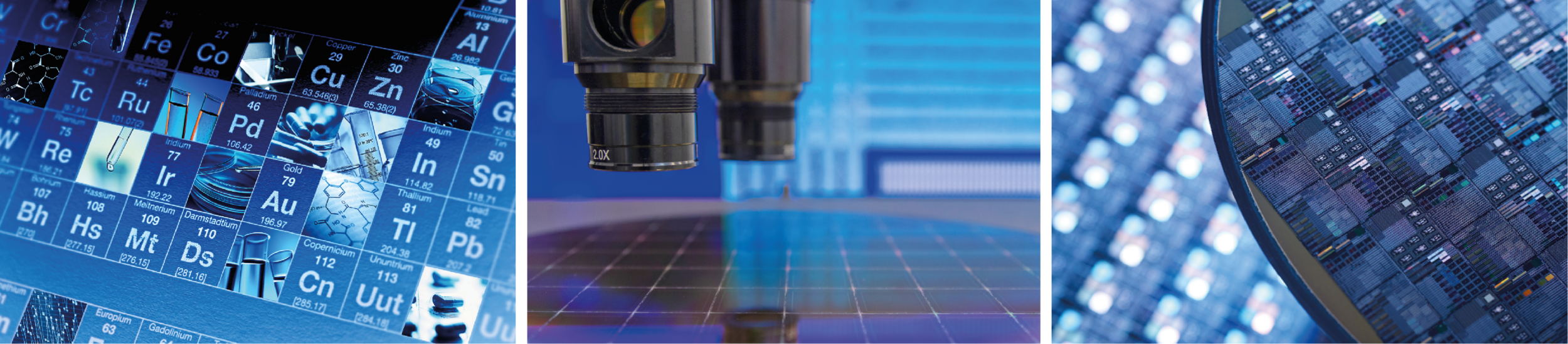
Thin Film characterization are important in the development phase of new materials to minimize the time to market of a new generation of devices and in the metrology step, which is required for improving the yield of a production line for minimizing wafer-to-wafer variation. HORIBA a leader in optical spectroscopy from deep UV to XRF offers a unique range of high-end tools for Materials and Thin Film Analysis which can used in R&D, In-Line or integrated in a process chamber.
Key Benefits:

Spectroscopic Ellipsometer from FUV to NIR: 190 to 2100 nm

In-situ spectroscopic ellipsometer for real-time thin film monitoring

Spectroscopic Ellipsometer for Simple Thin Film Measurement

AFM-Raman for Physical and Chemical imaging
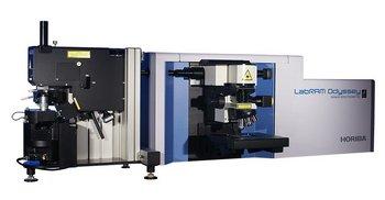
AFM-Raman for physical and chemical imaging

Camera Endpoint Monitor based on Real Time Laser Interferometry
Do you have any questions or requests? Use this form to contact our specialists.