There is a local version available of this page. Change to the local version?
United States

Semiconductors

Crystal Defect Analysis for Semiconductor Raw Materials

<< Back to Raw Materials for Semiconductors

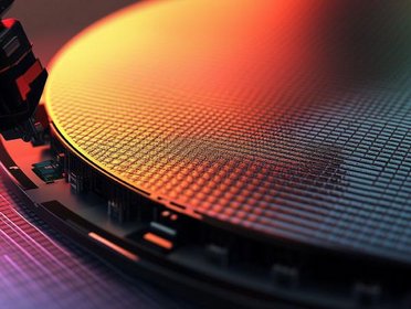
Reducing defects and precisely controlling impurities have become increasingly important in semiconductor devices for high-speed communication. We will introduce analysis cases illustrating this.

Cathodoluminescence measurement system HORIBA CLUE series

  • Can be added to existing electron microscopes
  • Compatible with measurements at ultraviolet to near-infrared wavelengths (200 to 2,100 nm)
  • SEM integrated high range CL imaging device (Imaging CL) can also be proposed.

AFM (atomic force microscope) Raman XploRA Nano

  • Acquire physical information by AFM and chemical information by Raman simultaneously
  • Stress distribution analysis on the outermost surface on the order of nm is possible.

Browse all applications related to Crystal defect analysis

Request for Information

Do you have any questions or requests? Use this form to contact our specialists.

* These fields are mandatory.