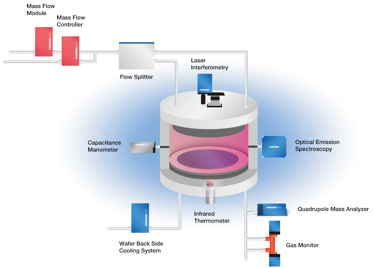
To reduce the chamber-to-chamber variation and to optimize the yield of an etching tool, HORIBA offers a wide range of fluid control modules and smart sensors for endpoint detection and chamber health monitoring. Compact and robust, they can be used for R&D and for Production.
蚀刻在微细制造中用于在制造过程中化学去除晶圆片表面的层。蚀刻是一个非常重要的工艺模块,每个晶圆在完成之前都要经过许多蚀刻步骤。
在许多蚀刻步骤中,晶圆片的一部分被一种抗蚀刻的“掩蔽”材料保护起来不受蚀刻剂的影响。在某些情况下,掩蔽材料是用光刻法制成的光刻胶。其他情况需要更耐用的掩膜,如氮化硅。
Dry etching refers to the removal of material, typically a masked pattern of semiconductor material, by exposing the material to a bombardment of ions (usually a plasma of reactive gases such as fluorocarbons, oxygen, chlorine, boron trichloride; sometimes with addition of nitrogen, argon, helium and other gases) that dislodge portions of the material from the exposed surface. A common type of dry etching is reactive-ion etching. Unlike with many (but not all, see isotropic etching) of the wet chemical etchants used in wet etching, the dry etching process typically etches directionally or anisotropically.
Wafer Back Side Cooling System
高响应压力非敏感质量流量器
宽范围压敏质量流量计
压差式质量流量控制器
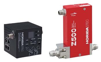
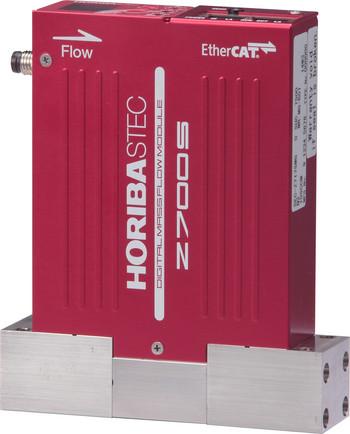
紧凑型质量流量控制器
热式气体分流器
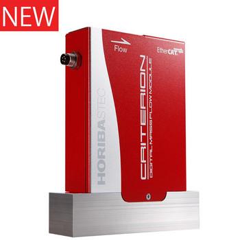
多量程/多气体数字质量流量控制器
新型压力补偿质量流量控制器
压力补偿质量流量控制器
直接液体注入系统
数字式液体质量流量计
压电阀
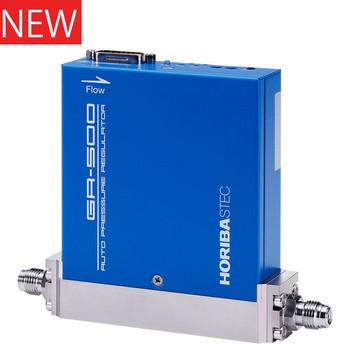
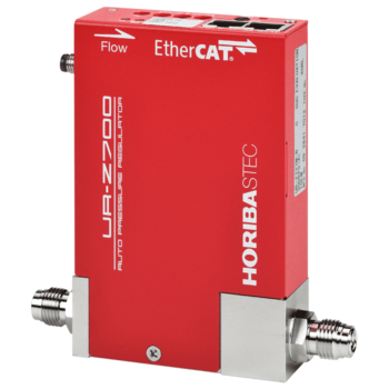
数字式自动压力调节器
晶圆背面冷却系统
HORIBA's expertise in analytical instrumentation has provided the foundations for a range of successful industrial monitoring tools for the semiconductor, pharmaceutical and chemical industries.
With its new compact design and enhanced image quality, the LEM interferometer for in-situ etch rate monitoring and end-point detection can be mounted on any process chamber with a direct top view of the wafer. It provides a real-time digital CCD image of the sample surface, making its 30-m laser beam positioning simple and accurate. Based on interferometry technique, the LEM provide in-situ etch/growth rate monitoring for endpoint detection of a wide range of dry etch applications.
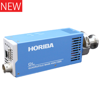
Quadrupole Mass Analyzer
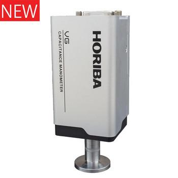
电容式压力计
基于光发射光谱和 MWL 干涉测量法的工艺终点/反应腔健康监测
光发射光谱蚀刻终点监测仪
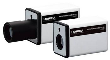
高精度红外温度计[固定式]
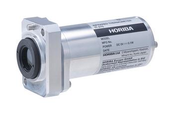
High-Accuracy Infrared Thermometer [Built-in type]
基于实时激光干涉测量的摄像头终点监测
等离子体发射控制器
如您有任何疑问,请在此留下详细需求信息,我们将竭诚为您服务。