技术及常见问题答疑
AFM-Raman (同区域测量和TERS)
TERS将拉曼光谱引入纳米级分辨率成像。进一步了解这种超分辨率化学成像技术。
本应用报告介绍了对电子束光刻法制造的石墨烯纳米带(GNRs)的TERS表征。TERS可实现的化学纳米尺度分辨率揭示了GNRs边缘的无定形碳的存在,并定位了有机残留物。TERS可以被认为是表征纳米石墨烯的一个有价值的工具,这是开发基于石墨烯的纳米设备的一个重要步骤。
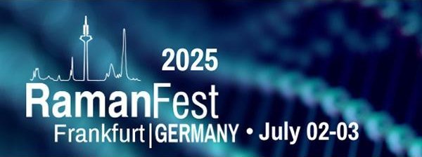
查看详情The 12th International Conference on Advanced Applied Raman Spectroscopy (RamanFest 2025) will feature presentations from world-leading Raman experts and researchers using the technique across varied applications within life science, materials science, and energy and environmental analysis. It will bring together the world's Raman community to share, learn and discuss how Raman spectroscopy is being applied to today's problems, and pioneering tomorrow's capabilities.
Read moreIn this webinar, a number of exciting developments in the tip-enhanced Raman spectroscopy (TERS) field will be discussed, including non–trivial excitation wavelength dependence of the gap-mode TERS response of transition metal dichalcogenides (TMDs) on silver that resulted in reconsidering the role of resonance effects and strong optical coupling in TERS and completely unexpected discovery of the normally forbidden Raman bands in TERS spectra of the monolayer h-BN on gold caused by the proximity of TMD monolayer to multiple layers exfoliated on top...
Watch it nowThe combination of Atomic Force Microscopy (AFM) and Raman spectroscopy provides deep insights into the complex properties of various materials. While Raman spectroscopy facilitates the chemical characterization of compounds, interfaces and complex matrices, offering crucial insights into molecular structures and compositions, including microscale contaminants and trace materials. AFM provides essential data on topography and mechanical properties, such as surface texture, adhesion, roughness, and stiffness at the nanoscale.
Watch it nowThe growing of semiconductor materials industrialization requires technologies to characterize their properties. Optical microspectroscopic platforms like Raman microscopes offer both physical and chemical information in one system. Thus, process qualification, wafer uniformity assessment, or defects inspection of wafers can be achieved with Raman microscopy. These can also be applied to new materials characterization.
In this webinar, we will highlight how Photoluminescence and Raman microscopies can address semiconductor challenges. We will also show how the combination of micro-spectroscopies with AFM (Atomic Force Microscopy) can provide nano resolution and deeper understanding of these structures.
Watch it nowTrue colocalized topographic, electrical, and chemical characterization of exfoliated graphene flakes
Graphene, a single layer of carbon atoms arranged in a two-dimensional honeycomb lattice, exhibits remarkable electrical, thermal, and mechanical properties, making it a subject of extensive research in various scientific fields.
Read moreTrue colocalized topographic, electrical, and chemical characterization of Van der Waals heterostructures
Van der Waals heterostructures, with their unique properties arising from the weak interlayer coupling and strong in-plane bonding, offer exciting opportunities for the design of novel materials with tailored electronic, optical, and mechanical properties.
Read more本应用报告了脂质纳米管(LNTs)作为碳模板用于制造纳米结构的TERS表征。据悉,这些脂质纳米管(LNTs)是最小的具有表面图案的有机模板。TERS成像能够以数十纳米的空间分辨率识别LNTs的化学特征。
查看详情Nanoscale chemical imaging of Single- to Few-Layer Ti₃C₂Tₓ MXene
MXenes is the largest and fastest growing 2D materials. They have unique properties such as good conductivity and a hydrophilic surface. The control of nanoscale composition would ultimately allow for engineering properties locally, gaining more control over the 2D material-based systems.
Read moreTERS Nano-localization of SERS hot spots
Surface-enhanced Raman scattering (SERS) is a powerful plasmonics-based analytical technique for biosensing. SERS effect relies on nanostructures that need to be designed to maximize enhancement factors and molecular specificity. In addition to numerical modeling, an analytical tool capable of imaging localized enhancement would be an added value.
Read more有机忆阻器的出现受到了低重复性、耐久性、可扩展性和低开关速度的阻碍。了解分子尺度上的主要驱动机制将是提高这种有机基器件的坚固性和可靠性的关键。
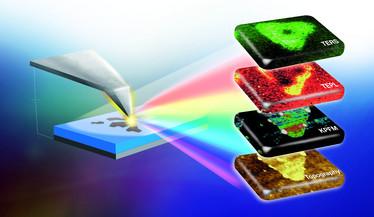
查看详情AFM-Raman及其TERS模式,以10nm的空间分辨率显示了氧化石墨烯(GO)片表面结构缺陷和化学基团的纳米图谱分析。TERS图谱与KPFM测量相结合,用于GO表面的实时形貌学、电学和化学成像。这种多参数测量方法扩展了TERS的应用能力,展示了纳米尺度上局部的化学成分和物理性质的直接相关性,这不仅仅适用于2D材料,它几乎可以适用于任何样品表面。
查看详情本应用案例揭示了侧面照明/收集方式术成功应用于测量液体中TERS研究的关键仪器细节。这种能力旨在为多相催化、电化学、细胞生物学和生物材料等许多应用带来突破。在这篇文章中,石墨烯氧化物薄片和碳纳米管浸入水中的纳米尺度化学成像与真正的非接触原子力显微镜图像一起显示优于20nm的高分辨能力。
查看详情道路机动车辆排放的低于23nm的颗粒物引起了人们对人类健康的新关注。除了测量粒子的数量和质量外,还必须确定纳米粒子的表面化学成分,以了解其与环境的潜在反应性。
查看详情本应用案例报道了未来纳米级电子和光电器件的高潜力半导体的二维材料(TMDCs)的纳米特性。扫描探针显微镜通过等离激元增强耦合光致发光(PL)和拉曼光谱技术,获得纳米尺度下的关键形貌信息和电子特性,从而产生纳米尺度下的相关电学和化学信息。
查看详情本篇应用文档报道了TERS 表征沉积在镀金衬底上的磷脂双分子层,该样品可以用作标准样品,检测到脂质成分在纳米尺度上的分布。此外,还引入了纳米材料来模拟纳米颗粒和细胞膜之间的相互作用,帮助更好地研究纳米材料对人类健康的毒性。 TERS 检测磷脂双分子层中纳米颗粒的灵敏度可以低至飞摩尔浓度,空间分辨率低至 7 nm。还开发了一种特定的液体样品池,可以实现在溶液中进行 TERS 测量,应用文档中提供了测试氧化石墨烯样品的结果。
查看详情本应用报告介绍了对电子束光刻法制造的石墨烯纳米带(GNRs)的TERS表征。TERS可实现的化学纳米尺度分辨率揭示了GNRs边缘的无定形碳的存在,并定位了有机残留物。TERS可以被认为是表征纳米石墨烯的一个有价值的工具,这是开发基于石墨烯的纳米设备的一个重要步骤。
查看详情The 12th International Conference on Advanced Applied Raman Spectroscopy (RamanFest 2025) will feature presentations from world-leading Raman experts and researchers using the technique across varied applications within life science, materials science, and energy and environmental analysis. It will bring together the world's Raman community to share, learn and discuss how Raman spectroscopy is being applied to today's problems, and pioneering tomorrow's capabilities.
Read moreIn this webinar, a number of exciting developments in the tip-enhanced Raman spectroscopy (TERS) field will be discussed, including non–trivial excitation wavelength dependence of the gap-mode TERS response of transition metal dichalcogenides (TMDs) on silver that resulted in reconsidering the role of resonance effects and strong optical coupling in TERS and completely unexpected discovery of the normally forbidden Raman bands in TERS spectra of the monolayer h-BN on gold caused by the proximity of TMD monolayer to multiple layers exfoliated on top...
Watch it nowThe combination of Atomic Force Microscopy (AFM) and Raman spectroscopy provides deep insights into the complex properties of various materials. While Raman spectroscopy facilitates the chemical characterization of compounds, interfaces and complex matrices, offering crucial insights into molecular structures and compositions, including microscale contaminants and trace materials. AFM provides essential data on topography and mechanical properties, such as surface texture, adhesion, roughness, and stiffness at the nanoscale.
Watch it nowThe growing of semiconductor materials industrialization requires technologies to characterize their properties. Optical microspectroscopic platforms like Raman microscopes offer both physical and chemical information in one system. Thus, process qualification, wafer uniformity assessment, or defects inspection of wafers can be achieved with Raman microscopy. These can also be applied to new materials characterization.
In this webinar, we will highlight how Photoluminescence and Raman microscopies can address semiconductor challenges. We will also show how the combination of micro-spectroscopies with AFM (Atomic Force Microscopy) can provide nano resolution and deeper understanding of these structures.
Watch it nowTrue colocalized topographic, electrical, and chemical characterization of exfoliated graphene flakes
Graphene, a single layer of carbon atoms arranged in a two-dimensional honeycomb lattice, exhibits remarkable electrical, thermal, and mechanical properties, making it a subject of extensive research in various scientific fields.
Read moreTrue colocalized topographic, electrical, and chemical characterization of Van der Waals heterostructures
Van der Waals heterostructures, with their unique properties arising from the weak interlayer coupling and strong in-plane bonding, offer exciting opportunities for the design of novel materials with tailored electronic, optical, and mechanical properties.
Read more本应用报告了脂质纳米管(LNTs)作为碳模板用于制造纳米结构的TERS表征。据悉,这些脂质纳米管(LNTs)是最小的具有表面图案的有机模板。TERS成像能够以数十纳米的空间分辨率识别LNTs的化学特征。
查看详情Nanoscale chemical imaging of Single- to Few-Layer Ti₃C₂Tₓ MXene
MXenes is the largest and fastest growing 2D materials. They have unique properties such as good conductivity and a hydrophilic surface. The control of nanoscale composition would ultimately allow for engineering properties locally, gaining more control over the 2D material-based systems.
Read moreTERS Nano-localization of SERS hot spots
Surface-enhanced Raman scattering (SERS) is a powerful plasmonics-based analytical technique for biosensing. SERS effect relies on nanostructures that need to be designed to maximize enhancement factors and molecular specificity. In addition to numerical modeling, an analytical tool capable of imaging localized enhancement would be an added value.
Read more有机忆阻器的出现受到了低重复性、耐久性、可扩展性和低开关速度的阻碍。了解分子尺度上的主要驱动机制将是提高这种有机基器件的坚固性和可靠性的关键。
查看详情AFM-Raman及其TERS模式,以10nm的空间分辨率显示了氧化石墨烯(GO)片表面结构缺陷和化学基团的纳米图谱分析。TERS图谱与KPFM测量相结合,用于GO表面的实时形貌学、电学和化学成像。这种多参数测量方法扩展了TERS的应用能力,展示了纳米尺度上局部的化学成分和物理性质的直接相关性,这不仅仅适用于2D材料,它几乎可以适用于任何样品表面。
查看详情本应用案例揭示了侧面照明/收集方式术成功应用于测量液体中TERS研究的关键仪器细节。这种能力旨在为多相催化、电化学、细胞生物学和生物材料等许多应用带来突破。在这篇文章中,石墨烯氧化物薄片和碳纳米管浸入水中的纳米尺度化学成像与真正的非接触原子力显微镜图像一起显示优于20nm的高分辨能力。
查看详情道路机动车辆排放的低于23nm的颗粒物引起了人们对人类健康的新关注。除了测量粒子的数量和质量外,还必须确定纳米粒子的表面化学成分,以了解其与环境的潜在反应性。
查看详情本应用案例报道了未来纳米级电子和光电器件的高潜力半导体的二维材料(TMDCs)的纳米特性。扫描探针显微镜通过等离激元增强耦合光致发光(PL)和拉曼光谱技术,获得纳米尺度下的关键形貌信息和电子特性,从而产生纳米尺度下的相关电学和化学信息。
查看详情本篇应用文档报道了TERS 表征沉积在镀金衬底上的磷脂双分子层,该样品可以用作标准样品,检测到脂质成分在纳米尺度上的分布。此外,还引入了纳米材料来模拟纳米颗粒和细胞膜之间的相互作用,帮助更好地研究纳米材料对人类健康的毒性。 TERS 检测磷脂双分子层中纳米颗粒的灵敏度可以低至飞摩尔浓度,空间分辨率低至 7 nm。还开发了一种特定的液体样品池,可以实现在溶液中进行 TERS 测量,应用文档中提供了测试氧化石墨烯样品的结果。
查看详情本应用报告介绍了对电子束光刻法制造的石墨烯纳米带(GNRs)的TERS表征。TERS可实现的化学纳米尺度分辨率揭示了GNRs边缘的无定形碳的存在,并定位了有机残留物。TERS可以被认为是表征纳米石墨烯的一个有价值的工具,这是开发基于石墨烯的纳米设备的一个重要步骤。
查看详情There are no results for this filter combination!
生物型纳米拉曼光谱仪

纳米拉曼光谱仪

纳米拉曼光谱仪

AFM光学工作站

先进原子力显微镜

多光路耦合纳米拉曼光谱仪

纳米拉曼光谱仪
如您有任何疑问,请在此留下详细需求信息,我们将竭诚为您服务。