There is a local version available of this page. Change to the local version?
United States

Semiconductors

Stress analysis of SiC

SiC combined analysis by Raman and CL

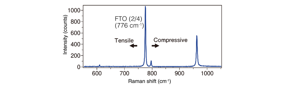
Residual stress in SiC is determined by peak shift amount of 776cm-1


Since the position of the defect in the cathodoluminescence (CL) image matches the position of the peak shift change, defects inside the wafer that cannot be seen in the CL image can be predicted from the Raman peak shift.

Microscopic Raman spectrometer LabRAM Odyssey

  • Industry's highest level* stress resolution (*according to our research in 2022)
  • Capable of mapping up to 12 inch wafers
  • Temperature control holder can be used (please consult us separately regarding sample size)


AFM (atomic force microscope) Raman XploRA Nano

  • Acquire physical information by AFM and chemical information by Raman simultaneously
  • Stress distribution analysis on the outermost surface on the order of nm is possible.

留言咨询

如您有任何疑问,请在此留下详细需求信息,我们将竭诚为您服务。

* 这些字段为必填项。

You might also like to know