<< Back to Raw Materials for Semiconductors
Silicon material continues to be mainstream of next-generation packages that integrate miniaturized chips and chiplets, making it possible to create more complex integrated systems as well as less expensive. HORIBA will contribute with its measurement technology for film thickness measurement, stress analysis, elemental analysis, and foreign material analysis of silicon materials.
Film Thickness and Quality | Stress Analysis | Elemental Analysis | Foreign Object Detection/Analysis
In the advancement of thin film technology through miniaturization, we propose solutions for achieving high film deposition control, such as in-situ evaluation during the film deposition process and evaluation of thin films at the Ångström order level.
Membrane information obtained using a spectroscopic ellipsometer
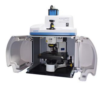
We propose a multifaceted stress evaluation solution using a Raman spectrometer boasting high wavenumber and spatial resolution, along with cathodoluminescence (CL).
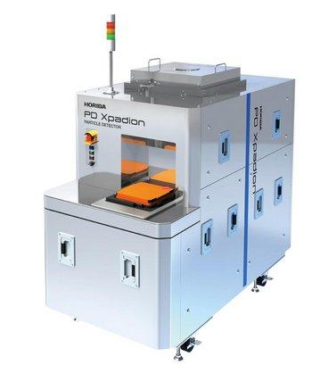
Defects in wafers can also be caused by foreign matter, and we will introduce a method of microscopic elemental analysis to identify the cause of defects.
如您有任何疑问,请在此留下详细需求信息,我们将竭诚为您服务。
研究级经典型椭偏仪
高分辨超灵敏智能拉曼成像仪
高性能全自动拉曼光谱
高速高分辨显微共焦拉曼光谱仪
纳米拉曼光谱仪
纳米拉曼光谱仪
碳/硫分析仪
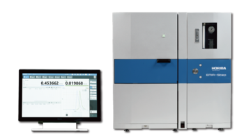
氧/氮/氢分析仪
氧/氮/氢分析仪
Reticle / Mask Particle Detection System