<< Back to Raw Materials for Semiconductors
Compound semiconductors are used as power devices under high current and voltage, and are also used as LEDs and high-performance optical sensors, taking advantage of their light-receiving and high-efficiency properties. They are also used as high-frequency devices in the telecommunications industry. This wide range of applications enhances the future potential of compound semiconductors. HORIBA contributes its measurement technology for film thickness measurement, defects analysis, carrier life analysis, and foreign matter analysis of compound semiconductors.
Film Thickness and Quality | Depth Elemental Profile Analysis | Crystal Defect Analysis | Foreign Object Detection/Analysis | Career Lifetime Analysis
In the advancement of thin film technology through miniaturization, HORIBA proposes solutions for achieving high film deposition control, such as in-situ evaluation during the film deposition process and evaluation of thin films at the Ångström order level.
Membrane information obtained using a spectroscopic ellipsometer
We introduce an analysis method that allows for the rapid and easy determination of the depth-directional distribution of elements in compound semiconductor thin films, where performance varies significantly depending on the composition ratio of elements.
Reducing defects and precisely controlling impurities have become increasingly important in semiconductor devices for high-speed communication. We will introduce analysis cases illustrating this.
Defects in wafers can also be caused by foreign matter, and we will introduce a method of microscopic elemental analysis to identify the cause of defects.
Deposition of highly crystalline SiC epitaxial films is essential for high-performance compound semiconductors, and we will introduce a non-destructive and precise method for analyzing crystallinity after deposition.
如您有任何疑问,请在此留下详细需求信息,我们将竭诚为您服务。
研究级经典型椭偏仪
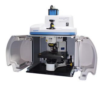
高分辨超灵敏智能拉曼成像仪
高性能全自动拉曼光谱
高速高分辨显微共焦拉曼光谱仪
纳米拉曼光谱仪
纳米拉曼光谱仪
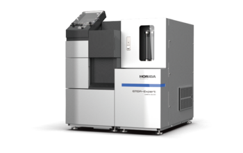
碳/硫分析仪
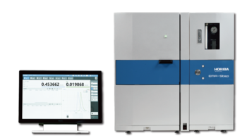
氧/氮/氢分析仪
氧/氮/氢分析仪
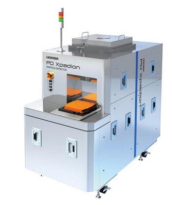
Reticle / Mask Particle Detection System


")