<< Back to Raw Materials for Semiconductors
Nanocarbon material (diamond, graphene, carbon nanotubes and so on) have excellent electrical properties, such as high electron mobility and tolerance to a high current density. They also have high thermal conductivity and mechanical strength, and are therefore promising materials for future electronic devices for a breakthrough. HORIBA contributes its measurement technology for film thickness measurement and defects analysis of nanocarbon materials.
Film Thickness and Quality | Stress Analysis | Elemental Analysis | Foreign Object Detection/Analysis
In the advancement of thin film technology through miniaturization, we propose solutions for achieving high film deposition control, such as in-situ evaluation during the film deposition process and evaluation of thin films at the Ångström order level.
Membrane information obtained using a spectroscopic ellipsometer
We propose a multifaceted stress evaluation solution using a Raman spectrometer boasting high wavenumber and spatial resolution, along with cathodoluminescence (CL).
Defects in wafers can also be caused by foreign matter, and we will introduce a method of microscopic elemental analysis to identify the cause of defects.
如您有任何疑问,请在此留下详细需求信息,我们将竭诚为您服务。
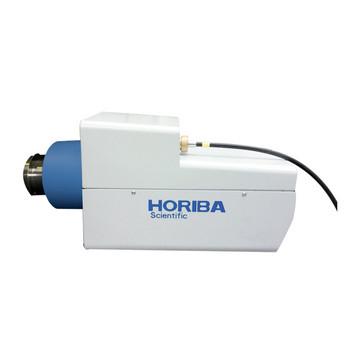
研究级经典型椭偏仪
拉曼光致荧光与阴极荧光
多功能高光谱阴极荧光
紧凑型高光谱阴极荧光
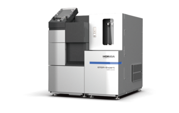
氧/氮/氢分析仪
氧/氮/氢分析仪
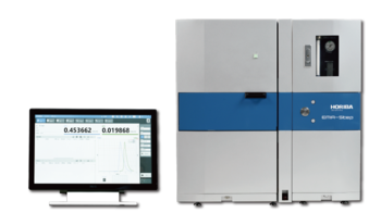
碳/硫分析仪
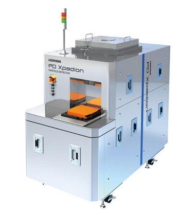
Reticle / Mask Particle Detection System