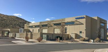
HORIBA, Ltd. (Head Office: Kyoto, Japan; hereinafter, “HORIBA”) announced today the relocation of a development site in Reno, Nevada, USA (hereinafter, the “Reno Technology Center”) with a view toward developing technology for fluid measurement and control of gases and liquids for the semiconductor production process. The new site will go into full operation on August 23, 2018. The Reno Technology Center is a branch of HORIBA’s subsidiary, HORIBA Instruments Incorporated (Headquarters: Irvine, California, USA), and performs research and development mainly for HORIBA STEC, Co., Ltd. (hereinafter, “STEC”). Fluid measurement and control of gases and liquids play a key role in the semiconductor production process, and related technological requirements are becoming increasingly advanced. In order to promptly respond to customer demands, it is vital to have an R&D site near key customers. Against this backdrop, it was decided to relocate and expand the office to enhance the development function, including both personnel and equipment.
By relocating the R&D function to a new, expanded site to reinforce development capability, HORIBA will remain committed to contributing to further development of the semiconductor industry.
Background to relocation of the Reno Technology Center
As more and more devices are connected to networks and communication volumes continue to surge, a variety of products, including not only mobile terminals, but also data centers and autonomous cars, are driving the semiconductor market forward. In recent years, the semiconductor memory market has been faring well, and semiconductor production equipment (SPE) manufacturers are making proactive capital expenditures in that market.
Fluid measurement and control of gases and liquids play a key role in the semiconductor production process, and the relevant technological requirements from customers are growing increasingly advanced as semiconductor devices continue to become miniaturized.
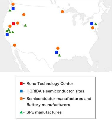
A number of SPE manufacturers have their development sites in North America, which makes it crucial to expand the development site there if HORIBA is to deepen relationships with customers and promptly meet their demands. With the aim of reinforcing the development function, which includes both personnel and equipment, it was decided to relocate and expand the office.
In July 2017, the gas mass flow calibration was certified for ISO/IEC 17025 at STEC’s Fukuchiyama Technology Center in Kyoto. Additionally, in May of this year, the Aso Factory in Kumamoto was expanded to double the production capacity of the company’s mainstay mass flow controllers. STEC remains committed to driving the semiconductor market by reinforcing development capability through relocation to the new site, while continuing to tap into the superior product quality and supply capacity that have been fostered in Japan.
Surroundings and Environment of Reno Technology Center
Semiconductor or SPE manufactures in USA are mostly based in Silicon Valley and other areas in the West Coast. Reno Technology Center is located with good access to these main manufacturers and is able to coordinate closely with HORIBA’s sales sites. Reno city is also the area with newly established industries, with large factories for the production of rechargeable batteries for electric vehicles being built in recent years.
In HORIBA’s research and development site, Reno, HORIBA continues to reinforce the cooperation upon not only HORIBA semiconductor but also other businesses.
About the new research site
Name: HORIBA Reno Technology Center
Location: 3740 Barron Way, Reno, Nevada 89511
Total floor area: 1,950m2
Development area: 1,700m2 (2.5 times larger than now)
Area of clean room: 148m2
Zoning: Office/development area
Building structure: Two-storied
Headcount: 38 (As of June 2018)
Hideyuki Koishi, President, STEC
“STEC set foot in Silicon Valley for the first time in 1989 when it established a sales office there for its mass flow controllers and other fluid measurement and control equipment. In North America, there are a particularly large number of semiconductor manufacturers that lead the global semiconductor market and SPE manufacturers that provide them with advanced processing, which makes it crucial for us to offer fast technological support. At the Reno Technology Center, our new development site, customer and market needs will be captured with even greater speed and accuracy to provide superior solutions. We will continue to reinforce its development capability on a global scale by accelerating collaborations with the development team in Japan and cooperation with application development teams in Europe, China, Taiwan, and South Korea, thereby contributing to further expansion of the semiconductor industry.”

